- 您现在的位置:买卖IC网 > Sheet目录988 > LP5521TMEV (National Semiconductor)EVAL BOARD FOR LP5521
�� ���
���
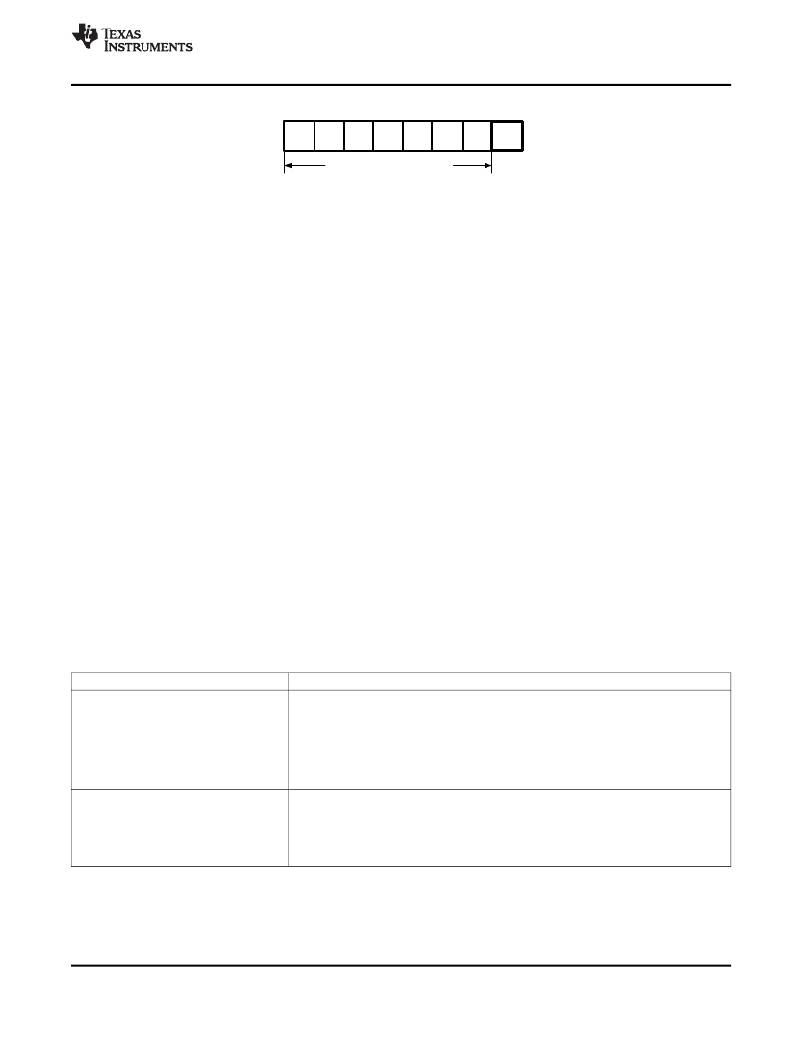
���MSB�
�SNVS441F� –� JANUARY� 2007� –� REVISED� FEBRUAY� 2013�
�LSB�
�ADR6�
�Bit7�
�ADR5�
�bit6�
�ADR4�
�bit5�
�ADR3�
�bit4�
�ADR2�
�bit3�
�ADR1�
�bit2�
�ADR0�
�bit1�
�R/W�
�bit0�
�2�
�I� C� SLAVE� address� (chip� address)�
�Figure� 31.� I� 2� C� chip� address�
�CONTROL� REGISTER� WRITE� CYCLE�
�?�
�?�
�?�
�?�
�?�
�?�
�?�
�?�
�?�
�Master� device� generates� start� condition.�
�Master� device� sends� slave� address� (7� bits)� and� the� data� direction� bit� (r/w� =� 0).�
�Slave� device� sends� acknowledge� signal� if� the� slave� address� is� correct.�
�Master� sends� control� register� address� (8� bits).�
�Slave� sends� acknowledge� signal.�
�Master� sends� data� byte� to� be� written� to� the� addressed� register.�
�Slave� sends� acknowledge� signal.�
�If� master� will� send� further� data� bytes� the� control� register� address� will� be� incremented� by� one� after�
�acknowledge� signal.�
�Write� cycle� ends� when� the� master� creates� stop� condition.�
�CONTROL� REGISTER� READ� CYCLE�
�?�
�?�
�?�
�?�
�?�
�?�
�?�
�?�
�?�
�?�
�?�
�Master� device� generates� a� start� condition.�
�Master� device� sends� slave� address� (7� bits)� and� the� data� direction� bit� (r/w� =� 0).�
�Slave� device� sends� acknowledge� signal� if� the� slave� address� is� correct.�
�Master� sends� control� register� address� (8� bits).�
�Slave� sends� acknowledge� signal.�
�Master� device� generates� repeated� start� condition.�
�Master� sends� the� slave� address� (7� bits)� and� the� data� direction� bit� (r/w� =� 1).�
�Slave� sends� acknowledge� signal� if� the� slave� address� is� correct.�
�Slave� sends� data� byte� from� addressed� register.�
�If� the� master� device� sends� acknowledge� signal,� the� control� register� address� will� be� incremented� by� one.� Slave�
�device� sends� data� byte� from� addressed� register.�
�Read� cycle� ends� when� the� master� does� not� generate� acknowledge� signal� after� data� byte� and� generates� stop�
�condition.�
�Address� Mode�
�<Start� Condition>�
�<Slave� Address><r/w� =� 0>[Ack]�
�<Register� Addr.>[Ack]�
�Data� Read�
�Data� Write�
�<Repeated� Start� Condition>�
�<Slave� Address><r/w� =� 1>[Ack]�
�[Register� Data]<Ack� or� NAck>�
�…� additional� reads� from� subsequent� register� address� possible�
�<Stop� Condition>�
�<Start� Condition>�
�<Slave� Address><r/w=’0’>[Ack]�
�<Register� Addr.>[Ack]�
�<Register� Data>[Ack]�
�…� additional� writes� to� subsequent� register� address� possible�
�<Stop� Condition>�
�Copyright� ?� 2007–2013,� Texas� Instruments� Incorporated�
�Product� Folder� Links:� LP5521�
��25�
�发布紧急采购,3分钟左右您将得到回复。
相关PDF资料
LPS0300H1000JB
RESISTOR HEAT SINK 100 OHM 300W
LPS0600H4R70JB
RESISTOR HEAT SINK 4.7 OHM 600W
LPS0800H1000JB
RESISTOR HEAT SINK 100 OHM 800W
LPS1100H47R0JB
RESISTOR HEAT SINK 47 OHM 1100W
LR1000
LINE CONDITIONER 1000W 4OUT
LR1200480D40R
RELAY SSR 40A 480VAC AC OUT PCB
LR2000
4NEMA & 3IEC-320 OUT LINE COND
LR604
LINE CONDITIONER 600W 3OUT
相关代理商/技术参数
LP5521TMX
制造商:NSC 制造商全称:National Semiconductor 功能描述:Programmable Three Channel LED Driver
LP5521TMX/NOPB
功能描述:LED照明驱动器 RoHS:否 制造商:STMicroelectronics 输入电压:11.5 V to 23 V 工作频率: 最大电源电流:1.7 mA 输出电流: 最大工作温度: 安装风格:SMD/SMT 封装 / 箱体:SO-16N
LP5521YQ
制造商:NSC 制造商全称:National Semiconductor 功能描述:Programmable Three Channel LED Driver
LP5521YQ/NOPB
功能描述:LED照明驱动器 3 Ch Prog Led Driver LLP RoHS:否 制造商:STMicroelectronics 输入电压:11.5 V to 23 V 工作频率: 最大电源电流:1.7 mA 输出电流: 最大工作温度: 安装风格:SMD/SMT 封装 / 箱体:SO-16N
LP5521YQ/S7002688
制造商:Rochester Electronics LLC 功能描述: 制造商:Texas Instruments 功能描述:
LP5521YQX
制造商:NSC 制造商全称:National Semiconductor 功能描述:Programmable Three Channel LED Driver
LP5521YQX/NOPB
功能描述:LED照明驱动器 RoHS:否 制造商:STMicroelectronics 输入电压:11.5 V to 23 V 工作频率: 最大电源电流:1.7 mA 输出电流: 最大工作温度: 安装风格:SMD/SMT 封装 / 箱体:SO-16N
LP5522
制造商:NSC 制造商全称:National Semiconductor 功能描述:Programmable LED Driver